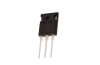


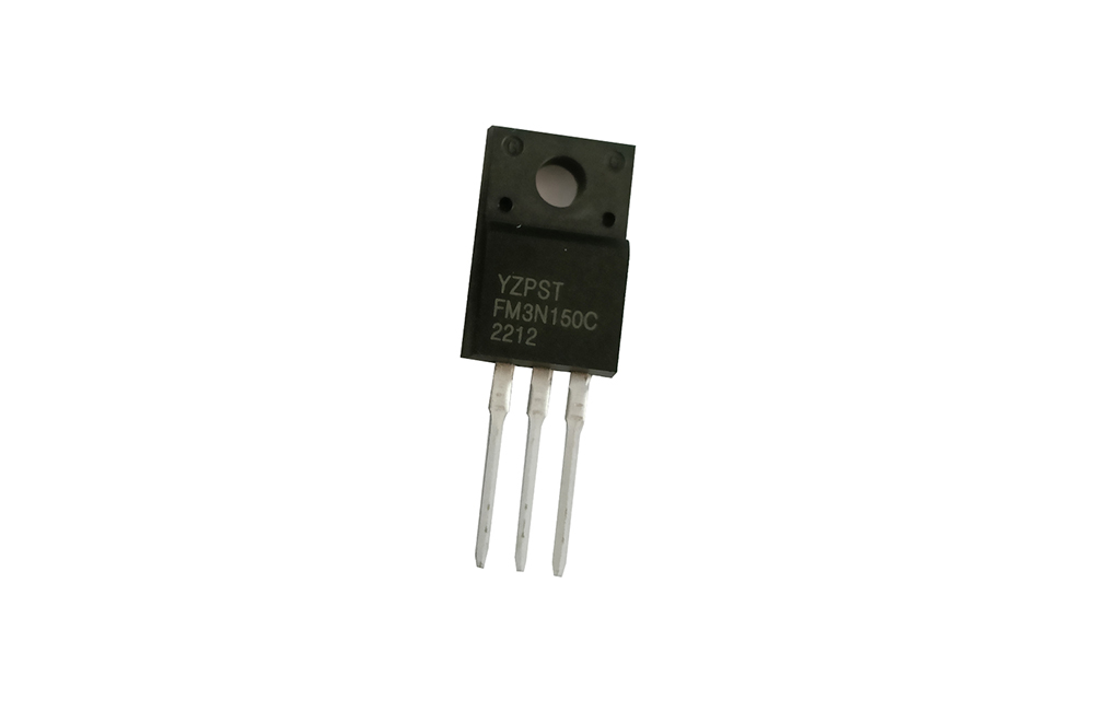
YZPST-FM3N150C


1500V N-Channel MOSFET
YZPST-FM3N150C
General Description
This Power MOSFET is produced using advanced self-aligned planar technology. This advanced technology has been especially tailored to minimize on-state resistance, provide superior switching performance, and withstand high energy pulse in the avalanche and commutation mode.
These devices can be used in various power switching circuit for system miniaturization and higher efficiency.
Features
3A, 1500V, RDS(on)typ. = 5Q@VGS = 10 V ld=1.5A
Low gate charge (typical9.3nC)
Low gate charge (typical2.4pf)
Fast switching
100% avalanche tested

Absolute Maximum Ratings Tc = 25 °C unless otherwise noted
| Symbol | Parameter | JFFM3N150C | Units | |
| Vdss | Drain - Source Voltage | 1500 | V | |
| Id | Drain Current | Continuous (Tc = 25 °C ) | 1.8 | A |
| Continuous ( Tc = 100 °C ) | 1.2 | A | ||
| Idm | Drain Current - Pulsed ( Note 1) | 12 | A | |
| Vgss | Gate - Source Voltage | ±30 | V | |
| EAS | Single Pulsed Avalanche Energy ( Note 2 ) | 225 | mJ | |
| dv/dt | Peak Diode Recovery dv/dt ( Note 3 ) | 5 | V/ns | |
| Pd | Power Dissipation (Tc = 25 °C ) | 30 | W | |
| Tj,Tstg | Operating and Storage Temperature Range | -55 to +150 | °C | |
| Tl | Maximum lead temperature for soldering purposes | 300 | °C | |
| 1/8〃 frome case for 5 seconds | ||||
Thermal characteristics
| Symbol | Parameter | JFFM3N150C | Units |
| Raic | Thermal Resistance, Junction-to-Case | 4.1 | °C/W |
| Rqja | Thermal Resistance, Junction-to-Ambient | 62.5 | °c/w |
Electrical Characteristics tc=25 °c unless otherwise noted
| Symbol | Parameter | Test Conditions | Min | Typ | Max | Units |
| Off Characteristics | ||||||
| BVdss | Drain - Source Breakdown Voltage | Vgs = 0 V, Id =250 uA | 1500 | ― | — | V |
| / BVdss/ | Breakdown Voltage Temperature Coefficient | Id = 250 uA, Referenced to | -- | 1.3 | -- | v/°c |
| 』Tj | 25 °C | |||||
| Zero Gate Voltage Drain Current | Vds = 1500 V, Vgs = 0 V | — | — | 25 | uA | |
| Idss | Vds = 1200 V, Tc = 125 °C | -- | -- | 500 | uA | |
| Igssf | Gate-Body Leakage Current, Forward | Vgs = 30 V, Vgs = 0 V | — | — | 100 | nA |
| Igssr | Gate-Body Leakage Current, Reverse | Vgs = -30 V, Vgs = 0 V | — | — | -100 | nA |
| On Characteristics | ||||||
| VGS(th) | Gate Threshold Voltage | Vds = Vgs, Id = 250 uA | 3 | — | 5 | V |
| RDS(on) | Static Drain-Source on-Resista nee | Vgs = 10 V, Id= 1.5A | — | 5 | 8 | Q |
| gFS | Forward Transconductance | Vds = 30 V, Id= 1.5 A ( Note | -- | 4.5 | -- | S |
| 4) | ||||||
| Dynamic Characteristics | ||||||
| Ciss | Input Capacitance | Vds = 25 V, Vgs = 0 V, f = | — | 1938 | — | pF |
| Coss | Output Capacitance | 1.0 MHz | — | 104 | — | pF |
| Crss | Reverse Transfer Capacitance | — | 2.4 | — | pF | |
| Rg | Gate resistance | F= 1.0 MHz | 3.5 | Q | ||
| Switching Characteristics | ||||||
| td(on) | Turn-On Delay Time | 34 | ns | |||
| tr | Turn-On Rise Time | Vds = 750 V, Id=3.0A/ Rg = | 17 | ns | ||
| td(off) | Turn-Off Delay Time | 100 , Vgs = 10 V (Note 4,5) | 56 | ns | ||
| tf | Turn-Off Fall Time | 27 | ns | |||
| Qe | Total Gate Charge | Vds = 750 V, Id =3.0 A Vgs = | 9.3 | nC | ||
| Qgs | Gate-Source Charge | 10 V (Note 4,5) | 15 | nC | ||
| Qgd | Gate-Drain Charge | 5.3 | nC | |||
| Drain - Source Diode Characteristics and Maximum Ratings | ||||||
| Is | Maximum Continuous Drain-Source Diode Forward Current | — | — | 3 | A | |
| Ism | Maximum Pulsed Drain-Source Diode Forward Current | — | — | 12 | A | |
| Vsd | Drain-Source Diode Forward Voltage | Vgs = 0 V, Is = 3.0 A | — | — | 1.5 | V |
| trr | Reverse Recovery Time | Vgs = 0 V, Is = 3.0 A | — | 302 | — | ns |
| Qrr | Reverse Recovery Charge | dlF/dt = 100 A/us ( Note | -- | 10 | -- | uC |
| 4) | ||||||
Notes:
1. Repetitive Rating : Pulsed width limited by maximum junction temperature
2. L= lO.OmH , Ias = 6.7A, Rg = 25Q, StartingTj = 25°C
3. Isd < 3.0Az di/dt < lOOA/us, Vdd < BVdss, Starting Tj = 25°C
4. Pulsed Test: Pulsed width <3OOusz Duty cycle < 2%
5. Essentially independent of operating temperature

For more information about YZPST-FM3N150C please download the PDF file above named " YZPST-FM3N150C"
Related Products