
.jpg?x-oss-process=image/resize,w_100/quality,q_100)
.jpg?x-oss-process=image/resize,w_100/quality,q_100)
.jpg?x-oss-process=image/resize,w_100/quality,q_100)


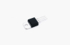
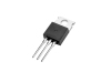
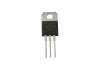
YZPST-Z0107MA


P/N:YZPST-Z0103MA; Z0103NA; Z0107MA; Z0107NA; Z0109MA; Z0109NA Z0103MN; Z0103NN; Z0107MN; Z0107NN; Z0109MN; Z0109NN
- Product profile
1.1 Description
Passivated triacs in conventional and surface mounting packages. Intended for use in applications requiring high bidirectional transient and blocking voltage capability.
Available in a range of gate current sensitivities for optimum performance.
Product availability:
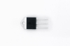
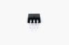
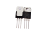
Z0103MA; Z0103NA; Z0107MA; Z0107NA; Z0109MA; Z0109NA in SOT54B Z0103MN; Z0103NN; Z0107MN; Z0107NN; Z0109MN; Z0109NN in SOT223.

1.2 Features
Blocking voltage to 800 V (NA and NN 1 A on-state RMS current. types)
1.3 Applications
Home appliances Small motor control
Fan controllers Small loads in industrial process control.
Pinning information
Table 1: Pinning - SOT54B (TO-92), SOT223, simplified outline and symbol
| 1 terminal 2 (T2) | SOT54B (TO-92) |
| 2 gate (G) | |
| 3 terminal 1 (T1) | |
| 1 terminal 1 (T1) SOT223 | |
| 2 | terminal 2 (T2) |
| 3 | gate (G) |
| 4 terminal 2 (T2) | |
3.1 Ordering options
Table 2: Ordering information
| Part Number | Voltage (VDRM) | Gate Sensitivity (IGT) | Package |
| Z0103MA | 600 V | 3 mA | SOT54B (TO-92) |
| Z0103NA | 800 V | 3 mA | SOT54B (TO-92) |
| Z0107MA | 600 V | 5 mA | SOT54B (TO-92) |
| Z0107NA | 800 V | 5 mA | SOT54B (TO-92) |
| Z0109MA | 600 V | 10 mA | SOT54B (TO-92) |
| Z0109NA | 800 V | 10 mA | SOT54B (TO-92) |
| Z0103MN | 600 V | 3 mA | SOT223 |
| Z0103NN | 800 V | 3 mA | SOT223 |
| Z0107MN | 600 V | 5 mA | SOT223 |
| Z0107NN | 800 V | 5 mA | SOT223 |
| Z0109MN | 600 V | 10 mA | SOT223 |
| Z0109NN | 800 V | 10 mA | SOT223 |
- Limiting values
Table 3: Limiting values
In accordance with the Absolute Maximum Rating System (IEC 60134).
| Symbol | Parameter | Conditions | Min |
Max | Unit |
| V DRM | repetitive peak off-state voltage | 25 °C ≤ Tj ≤ 125 °C | |||
| Z0103/07/09MA; Z0103/07/09MN | - | 600 | V | ||
| Z0103/07/09NA; Z0103/07/09NN | - | 800 | V | ||
| VRRM | repetitive peak reverse voltage | 25 °C ≤ Tj ≤ 125 °C | |||
| Z0103/07/09MA; Z0103/07/09MN | - | 600 | V | ||
| Z0103/07/09NA; Z0103/07/09NN | - | 800 | V | ||
| ITSM | non-repetitive peak on-state current | full sine wave; Tj = 25 °C prior to surge; | |||
| Figure 2 and Figure 3 | |||||
| t = 20 ms | - | 8 | A | ||
| t = 16.7 ms | - | 8.5 | A | ||
| IT(RMS) | RMS on-state current | all conduction angles; Figure 4 | |||
| SOT223 | Tsp = 90 °C | - | 1 | A | |
| SOT54B (TO-92) | T lead = 50 °C | - | 1 | A | |
| I2t | I2t for fusing | t = 10 ms | - | 0.35 | A2s |
| dIT/dt | rate of rise of on-state current | ITM = 1.0 A; IG = 2 x I GT; dIG/dt = 100 mA/µs | - | 20 | A/µs |
| IGM | peak gate current | tp = 20 µs | - | 1 | A |
| PGM | peak gate power | - | 2 | W | |
| PG(AV) | average gate power | over any 20 ms period | - | 0.1 | W |
| Tstg | storage temperature | −40 | 150 | °C | |
| Tj | junction temperature | −40 | 125 | °C |
Thermal characteristics
| Symbol | Parameter | Conditions | Min | Typ | Max | Unit |
| Rth(j-sp) | thermal resistance from junction to solder point for SOT223 | Figure 5 | - | - | 25 | K/W |
| Rth(j-lead) | thermal resistance from junction to lead for SOT54B (TO-92) | Figure 5 | - | - | 60 | K/W |
| Rth(j-a) | thermal resistance from junction to ambient | |||||
| SOT223 | minimum footprint; mounted on a PCB | - | 60 | - | K/W | |
| SOT54B (TO-92) | vertical in free air | - | 150 | - | K/W |
Characteristics
Tj= 25 ℃ unless otherwise .
| Symbol | Parameter | Conditions | Min | Typ | Max | Unit | |
| Static characteristics | |||||||
| I GT | gate trigger current | VD = 12 V; RL = 30 Ω; T2+ G+; T2+ G−; T2− G−; | |||||
| Z0103MA/MN/NA/NN | Figure 9 | - | - | 3 | mA | ||
| Z0107MA/MN/NA/NN | - | - | 5 | mA | |||
| Z0109MA/MN/NA/NN | - | - | 10 | mA | |||
| Z0103MA/MN/NA/NN | VD = 12 V; RL = 30 Ω; T2− G+; Figure 9 | - | - | 5 | mA | ||
| Z0107MA/MN/NA/NN | - | - | 7 | mA | |||
| Z0109MA/MN/NA/NN | - | - | 10 | mA | |||
| IL | latching current | VD = 12 V; RL = 30 Ω; T2+ G+; T2− G−; T2− G+; | |||||
| Z0103MA/MN/NA/NN | Figure 7 | - | - | 7 | mA | ||
| Z0107MA/MN/NA/NN | - | - | 10 | mA | |||
| Z0109MA/MN/NA/NN | - | - | 15 | mA | |||
| Z0103MA/MN/NA/NN | VD = 12 V; RL = 30 Ω; T2+ G− ; Figure 7 | - | - | 15 | mA | ||
| Z0107MA/MN/NA/NN | - | - | 20 | mA | |||
| Z0109MA/MN/NA/NN | - | - | 25 | mA | |||
| IH | holding current | IT = 50 mA; Figure 8 | |||||
| Z0103MA/MN/NA/NN | - | - | 7 | mA | |||
| Z0107MA/MN/NA/NN | - | - | 10 | mA | |||
| Z0109MA/MN/NA/NN | - | - | 10 | mA | |||
| VT | on-state voltage | Figure 6 | - | 1.3 | 1.6 | V | |
| VGT | gate trigger voltage | VD = 12 V; RL = 30 Ω; Tj = 25 。C; Figure 11 | - | - | 1.3 | V | |
| VD = V DRM; RL = 3.3 kΩ; Tj = 125 。C; Figure 11 | 0.2 | - | - | V | |||
| ID | off-state leakage current | VD = V DRM(max); VR = VRRM(max); Tj = 125 。C | - | - | 500 | μA | |
| Dynamic characteristics | |||||||
| dVD/dt | critical rate of rise of | VD = 0.67 V DRM(max); Tj = 110 。C; exponential waveform; gate open; Figure 10 | |||||
| off-state voltage | |||||||
| Z0103MA/MN/NA/NN | 10 | - | - | V/μs | |||
| Z0107MA/MN/NA/NN | 20 | - | - | V/μs | |||
| Z0109MA/MN/NA/NN | 50 | - | - | V/μs | |||
| dVcom/dt | critical rate of change of commutating voltage | VD = 400 V; IT = 1 A; Tj = 110 。C; | |||||
| Z0103MA/MN/NA/NN | dIcom/dt = 0.44 A/ms; gate open | 0.5 | - | - | V/μs | ||
| Z0107MA/MN/NA/NN | 1 | - | - | V/μs | |||
| Z0109MA/MN/NA/NN | 2 | - | - | V/μs | |||
lastic single-ended leaded (through hole) package; 3 leads

Related Products