
.jpg?x-oss-process=image/resize,w_100/quality,q_100)
.jpg?x-oss-process=image/resize,w_100/quality,q_100)
.jpg?x-oss-process=image/resize,w_100/quality,q_100)
.jpg?x-oss-process=image/resize,w_100/quality,q_100)
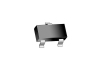
YZPST-D100H065AT1S3
Trench Field-Stop Technology IGBT
YZPST-D100H065AT1S3
Features
650V, 100A
VCE(sat)(typ.) =1.75V@VGE=15V, IC=100A
Maximum Junction Temperature 175
Pb-free Lead Plating; RoHS Compliant
Applications
Solar Converters
Uninterrupted Power Supply
Welding Converters
Mid to High Range Switching Frequency Converters
.jpg)


Trench Field-Stop Technology IGBT
YZPST-D100H065AT1S3
Features
650V, 100A
VCE(sat)(typ.) =1.75V@VGE=15V, IC=100A
Maximum Junction Temperature 175
Pb-free Lead Plating; RoHS Compliant
Applications
Solar Converters
Uninterrupted Power Supply
Welding Converters
Mid to High Range Switching Frequency Converters
Key Performance and Package Parameters
|
Order codes |
VCE |
IC |
VCEsat, Tvj=25 |
Tvjmax |
Marking |
Package |
|
D100H065AT1S3 |
650V |
100A |
1.75V |
175 ℃ |
D100H65AT1 |
TO247-3L |
Absolute Maximum Ratings
| Symbol | Parameter | Value | Unit |
| VCES | Collector-Emitter Voltage | 650 | V |
| VGES | Gate-Emitter Voltage | ±20 | V |
| IC | Continuous Collector Current (TC=25 ℃ ) | 125 | A |
| Continuous Collector Current (TC=100 ℃ ) | 100 | A | |
| ICM | Pulsed Collector Current (Note 1) | 200 | A |
| Diode Forward Current (TC=25 ℃ ) | 125 | A | |
| IF | Diode Forward Current (TC=100 ℃ ) | 100 | A |
| Maximum Power Dissipation (TC=25 ℃ ) | 385 | W | |
| PD | Maximum Power Dissipation (TC=100 ℃ ) | 192 | W |
| TJ | Operating Junction Temperature Range | -40 to 175 | ℃ |
| TSTG | Storage Temperature Range | -55 to 150 | ℃ |
Electrical Characteristics (Tc=25 unless otherwise noted.)
| Symbol | Parameter | Conditions | Min. | Typ. | Max. | Unit |
| BVCES | Collector-Emitter | VGE=0V, IC=200uA | 650 | V | ||
| Breakdown Voltage | --- | --- | ||||
| ICES | Collector-Emitter Leakage Current | VCE=650V, VGE=0V | 1 | mA | ||
| --- | --- | |||||
| Gate Leakage Current, Forward | VGE=20V, VCE=0V | 600 | nA | |||
| --- | --- | |||||
| IGES | Gate Leakage Current, Reverse | VGE=-20V, VCE=0V | 600 | nA | ||
| --- | --- | |||||
| VGE(th) | Gate Threshold Voltage | VGE=VCE , IC=750uA | 4.2 | --- | 6 | V |
| VCE(sat) | Collector-Emitter | VGE=15V, IC=100A, Tj=25 ℃ | --- | 1.75 | 2.2 | V |
| Saturation Voltage | VGE=15V, IC=100A, Tj=125 ℃ | --- | 2.05 | --- | V | |
| td(on) | Turn-on Delay Time | --- | 35 | --- | ns | |
| tr | Turn-on Rise Time | VCC=400V | --- | 155 | --- | ns |
| td(off) | Turn-off Delay Time | VGE=±15V | --- | 188 | --- | ns |
| tf | Turn-off Fall Time | IC=100A | --- | 69 | --- | ns |
| Eon | Turn-on Switching Loss | RG=8 | --- | 4.35 | --- | mJ |
| Eoff | Turn-off Switching Loss | Inductive Load | --- | 1.11 | --- | mJ |
| Ets | Total Switching Loss | TC=25 ℃ | --- | 5.46 | --- | mJ |
| Cies | Input Capacitance | VCE=25V | --- | 7435 | --- | pF |
| Coes | Output Capacitance | VGE=0V | --- | 237 | --- | pF |
| Cres | Reverse Transfer | f =1MHz | 128 | pF | ||
| Capacitance | --- | --- |
| Symbol | Parameter | Conditions | Min. | Typ. | Max. | Unit |
| IF=100A, Tj=25 ℃ | --- | 1.65 | 2.2 | V | ||
| VF | Diode Forward Voltage | IF=100A, Tj=150 ℃ | --- | 1.4 | --- | V |
| trr | Diode Reverse Recovery Time | 201 | ns | |||
| VR=400V | --- | --- | ||||
| IF=100A | ||||||
| Irr | Diode peak Reverse | dIF/dt=200A/us | 19 | A | ||
| Recovery Current | TC=25 ℃ | --- | --- | |||
| Qrr | Diode Reverse Recovery Charge | 2.45 | uC | |||
| --- | --- |
Note1 Repetitive rating, pulse width limited by maximum junction temperature
Package Information
.jpg)
Related Products