

.jpg?x-oss-process=image/resize,w_100/quality,q_100)
.jpg?x-oss-process=image/resize,w_100/quality,q_100)
.jpg?x-oss-process=image/resize,w_100/quality,q_100)
.jpg?x-oss-process=image/resize,w_100/quality,q_100)
YZPST-M2A016120L

N-Channel SiC Power MOSFET P/N: YZPST-M2A016120L
Features
High Blocking Voltage with Low On-Resistance
High Speed Switching with Low Capacitance
Easy to Parallel and Simple to Drive
Benefits
Higher System Efficiency
Reduced Cooling Requirements
Increased Power Density
Increased System Switching Frequency
Applications
Renewable Energy
EV Battery Chargers
High Voltage DC/DC Converters
Switch Mode Power Supplies
.jpg)

N-Channel SiC Power MOSFET P/N: YZPST-M2A016120L
Features
High Blocking Voltage with Low On-Resistance
High Speed Switching with Low Capacitance
Easy to Parallel and Simple to Drive
Benefits
Higher System Efficiency
Reduced Cooling Requirements
Increased Power Density
Increased System Switching Frequency
Applications
Renewable Energy
EV Battery Chargers
High Voltage DC/DC Converters
Switch Mode Power Supplies
Package
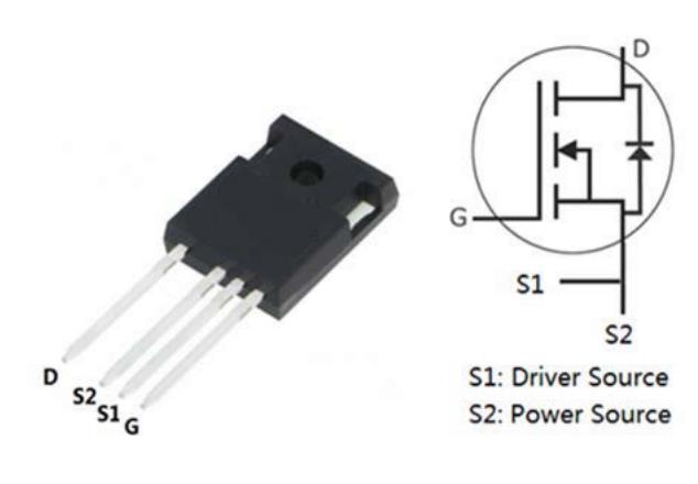
|
Part Number |
Package |
|
M2A016120L |
TO-247-4 |
Maximum Ratings (TC=25℃ unless otherwise specified)
| Symbol | Parameter | Value | Unit | Test Conditions | Note |
| VDSmax | Drain-Source Voltage | 1200 | V | VGS=0V, ID=100μA | |
| VGSmax | Gate-Source Voltage | -8/+22 | V | Absolute maximum values | |
| VGSop | Gate-Source Voltage |
-4/+18 |
V | Recommended operational values | |
| ID | Continuous Drain Current | 115 | A | VGS=18V, Tc=25℃ | |
| 76 | VGS=18V, Tc=100℃ | ||||
| ID(pulse) | Pulsed Drain Current | 250 | A | Pulse width tp limited by TJmax | |
| PD | Power Dissipation | 582 | W | Tc=25℃, TJ=175℃ | |
| TJ, TSTG | Operating Junction and Storage Temperature | -55 to +175 | ℃ |
Electrical Characteristics (TC=25℃ unless otherwise specified)
| Symbol | Parameter | Min. | Typ. | Max. | Unit | Test Conditions | Note |
| V(BR)DSS | Drain-Source Breakdown Voltage | 1200 | / | / | V | VGS=0V, ID=100μA | |
| VGS(th) | Gate Threshold Voltage | 1.9 | 2.6 | 4 | V | VDS=VGS, ID=23mA | |
| / | 1.8 | / | VDS=VGS, ID=23mA, TJ=175℃ | ||||
| IDSS | Zero Gate Voltage Drain Current | / | 1 | 100 | µA | VDS=1200V, VGS=0V | |
| IGSS+ | Gate-Source Leakage Current | / | 10 | 250 | nA | VDS=0V, VGS=22V | |
| IGSS- | Gate-Source Leakage Current | / | 10 | 250 | nA | VDS=0V, VGS=-8V | |
| RDS(on) | Drain-Source On-State Resistance | / | 16 | 21 | mΩ | VGS=18V, ID=75A | |
| / | 28 | / | VGS=18V, ID=75A, TJ=175℃ | ||||
| gfs | Transconductance | / | 40.5 | / | S | VDS=20V, ID=75A | |
| / | 37 | / | VDS=20V, ID=75A, TJ=175℃ | ||||
| Ciss | Input Capacitance | / | 4300 | / | VGS=0V | ||
| Coss | Output Capacitance | / | 236 | / | pF | VDS=1000V | |
| Crss | Reverse Transfer Capacitance | / | 35 | / | f=1MHz | ||
| Eoss | Coss Stored Energy | / | 136 | / | µJ | VAC=25mV | |
| EON | Turn-On Switching Energy | / | 2.1 | / | µJ | VDS=800V, VGS=-4V/18V | |
| EOFF | Turn-Off Switching Energy | / | 1.6 | / | ID=40A, RG(ext)=2.5Ω, L=100μH | ||
| td(on) | Turn-On Delay Time | / | 150 | / | |||
| tr | Rise Time | / | 38 | / | VDS=800V, VGS=-4V/18V, ID=40A RG(ext)=2.5Ω, RL=20Ω | ||
| td(off) | Turn-Off Delay Time | / | 108 | / | ns | ||
| tf | Fall Time | / | 35 | / | |||
| RG(int) | Internal Gate Resistance | / | 2.3 | / | Ω | f=1MHz, VAC=25mV | |
| QGS | Gate to Source Charge | / | 60 | / | VDS=800V | ||
| QGD | Gate to Drain Charge | / | 44 | / | nC | VGS=-4V/18V | |
| QG | Total Gate Charge | / | 242 | / | ID=40A |
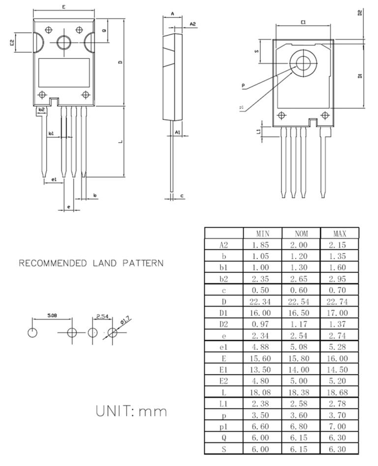
Package Dimensions
Related Products