


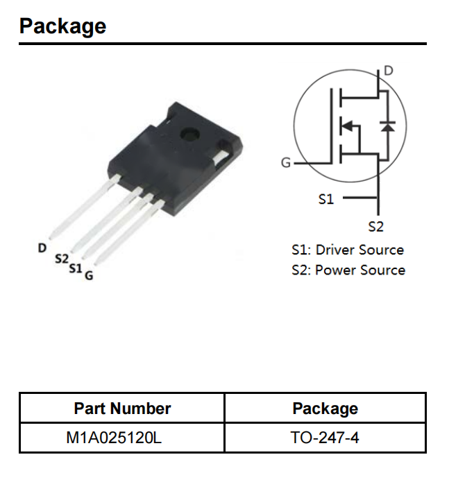
YZPST-M1A025120L
YZPST-M1A025120L
N-Channel SiC Power MOSFET
Features
High Blocking Voltage with Low On-Resistance
High Speed Switching with Low Capacitance
Easy to Parallel and Simple to Drive
Benefits
Higher System Efficiency
Reduced Cooling Requirements
Increased Power Density
Increased System Switching Frequency
Applications
Power Supplies
High Voltage DC/DC Converters
Motor Drives
Switch Mode Power Supplies
Pulsed Power applications
Maximum Ratings (TC=25℃ unless otherwise specified)
| Symbo | Parameter | Value | Unit | TestConditions | Note |
| VDSmax | Drain-SourceVoltage | 1200 | V | VGS=0V,ID=100μA | |
| VGSmax | Gate-SourceVoltage | -0.4 | V | Absolutemaximumvalues | |
| VGSop | Gate-SourceVoltage | -0.25 | V | Recommendedoperationalvalues | |
| ID | ContinuousDrain Current | 65 | A | VGS=20V,Tc=25C | |
| 43 | VGS=20V,Tc=100C | ||||
| ID(pulse) | Pulsed DrainCurrent | 200 | A | Pulse width tplimited byTJmax | |
| PD | PowerDissipation | 370 | W | Tc=25C,TJ=150C | |
| TJ, TSTG | OperatingJunction andStorage | -55 to+150 | C | ||
| Temperature |
Electrical Characteristics (TC=25C unlessotherwise specified)
| Symbol | Parameter | Min. | Typ. | Max. | Unit | TestConditions | Note |
| V(BR)DSS | Drain-SourceBreakdownVoltage | 1200 | / | / | V | VGS=0V,ID=100μA | |
| VGS(th) | GateThresholdVoltage | 1.9 | 2.4 | 4 | V | VDS=VGS,ID=15mA | Fig.11 |
| / | 1.7 | / | VDS=VGS,ID=15mA,TJ=150C | ||||
| IDSS | Zero GateVoltageDrainCurrent | / | 1 | 100 | µA | VDS=1200V,VGS=0V | |
| IGSS+ | Gate-SourceLeakageCurrent | / | 10 | 250 | nA | VDS=0V,VGS=25V | |
| IGSS- | Gate-SourceLeakageCurrent | / | 10 | 250 | nA | VDS=0V,VGS=-10V | |
| RDS(on) | Drain-SourceOn-StateResistance | / | 25 | 34 | mΩ | VGS=20V,ID=50A | Fig. |
| / | 43 | / | VGS=20V,ID=50A,TJ=150C | 4,5,6 | |||
| Ciss | InputCapacitance | / | 4200 | / | VGS=0V | Fig. | |
| Coss | OutputCapacitance | / | 250 | / | pF | VDS=1000V | 15,16 |
| Crss | ReverseTransferCapacitance | / | 16 | / | f=1MHz | ||
| Eoss | Coss StoredEnergy | / | 126 | / | µJ | VAC=25mV | |
| EON | Turn-OnSwitchingEnergy | / | 1.8 | / | J | VDS=800V,VGS=-5V/20VID=50A,RG(ext)=2.5Ω,L=412μH | |
| EOFF | Turn-OffSwitchingEnergy | / | 0.6 | / | |||
| td(on) | Turn-OnDelay Time | / | 15 | / | |||
| tr | Rise Time | / | 12 | / | ns | VDS=800V,VGS=-5V/20V,ID=50ARG(ext)=2.5Ω,RL=16Ω | |
| td(off) | Turn-OffDelay Time | / | 34 | / | |||
| tf | Fall Time | / | 7 | / | |||
| RG(int) | Internal GateResistance | / | 2.1 | / | Ω | f=1MHz,VAC=25mV | |
| GS | Gate toSourceCharge | / | 54 | / | VDS=800V | ||
| GD | Gate toDrain Charge | / | 29 | / | nC | VGS=-5V/20V | |
| G | Total GateCharge | / | 195 | / | ID=50A |
If you have any other inquiries for similar SiC Products, please contact us now.
We will provide you our full list for SiC Products.
Related Products

