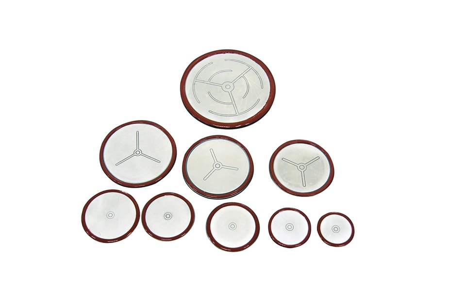
YZPST-KP Series-KP55
Tip: include the part number, target voltage/current and application environment.
Downloads & technical files

Chip Phase Control Thyristor 1600v-55mm
Symbol | Characteristic | Conditions | Temperature | Value | |
1 | VDRM | Repetitive peak off state voltage | -30°C£ Tj £125°C | 1600 | |
2 | VDSM | Non repetitive peak off state voltage | -30°C£ Tj £125°C | 1700 | |
3 | VRRM | Repetitive peak reverse voltage | -30°C£ Tj £125°C | 1600 | |
4 | VRSM | Non repetitive peak reverse voltage | -30°C£ Tj £125°C | 1700 | |
5 | IDRM | Repetitive peak off state current | V=VDRM | Tj = 125°C | ≤ 70 mA |
6 | IRRM | Repetitive peak reverse current | V=VRRM | Tj = 125°C | ≤ 70 mA |
7 | ITSM | Peak surge(non repetitive) current | Sinewave,10ms withoutreverse voltage | Tj = 125°C | 36.0 kA |
8 | VTO | Threshold voltage | Tj = 125°C | 0.82V | |
9 | Rt | On-state slope resistance | Tj = 125°C | 0.180 mohm | |
10 | VT | On-state voltage | IT = 2500 A | Tj = 125°C | ≤ 1.45V |
11 | VT | On-state voltage | IT = 3500 A | Tj = 125°C | ≤ 1.65V |
12 | DI/DT | Critical rate of rise of on-state current, min. |
From 75% VDRM
up to 1650 A, gate
10V 5ohm
| Tj = 125°C | 200 A / μ s |
13 | DV/DT | Critical rate of rise of off-state voltage, min. |
Linear ramp up
VD = 70 % VDRM
| Tj = 125°C | 500 V / μ s |
14 | IH | Holding current, typical |
VD=5V,
gate open circuit
| Tj = 25°C | ≤ 300 mA |
15 | IL | Latching current, typical |
VD=5V,
Tp=30 μs
| Tj = 25°C | ≤ 700 m A |
16 | VGT | Gate trigger voltage | VD= 5V; | Tj = 25°C | ≤ 3.0 V |
17 | IGT | Gate trigger current | VD= 5V; | Tj = 25°C | ≤ 200 m A |
18 | VGD | Non-trigger gate voltage, min. | VD= VDRM | Tj = 125°C | ≥ 0.25 V |
19 | PGM | Peak gate power dissipation | Tj = 25°C | 150W | |
20 | VFGM | Peak gate voltage (forward) | Tj = 25°C | 30V | |
21 | IFGM | Peak gate current | Tj = 25°C | 10 A | |
22 | VRGM | Peak gate voltage (reverse) | Tj = 25°C | 5V |
Ф A | Chip diameter | 55 mm |
Ф B |
External Emitter Contactdiameter = molybdenum washer
external diameter
| 45~46mm |
Ф C | Internal Emitter contac area =molybdenum washer internal | 8.5~8.6mm |
D | Chip thickness | 2.4~2.7mm |
E | Junction coating rubbermaxumum thickness | 0.2~0.4mm |
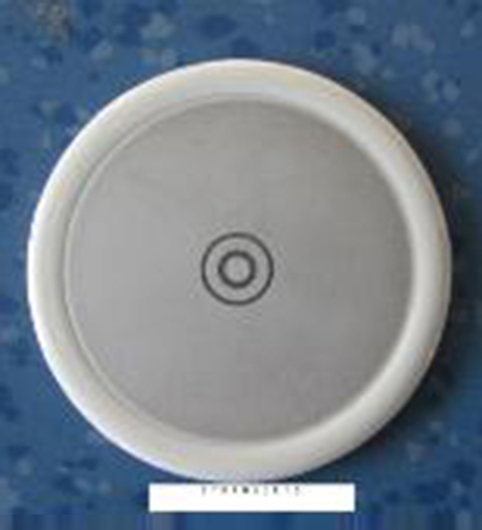
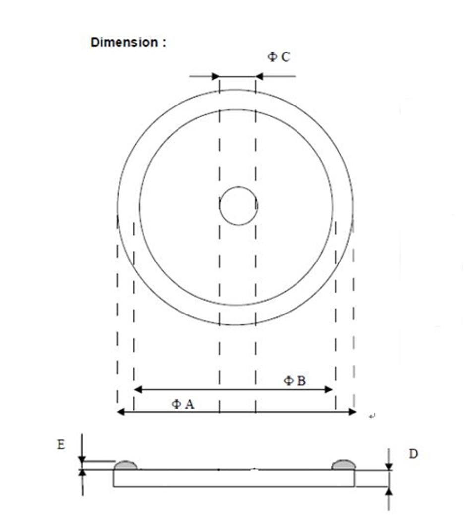
This outline is for 55mm SCR fusion element.
Junction have double Overcoats, the outside is Red.
Cathode Surface Metal:10~15um Aluminium.
Anode surface Metal:molybdenum
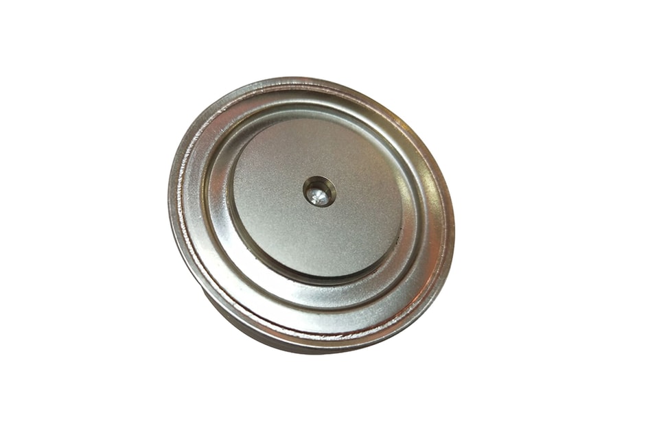
.jpg)

Power semiconductor devices, protection components and industrial power solutions.


