


.jpg?x-oss-process=image/resize,w_100/quality,q_100)


YZPST-RGN150C066


.jpg)
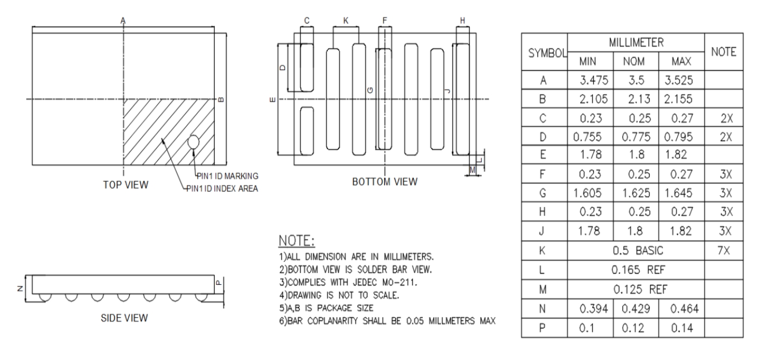
Pin information
|
PIN |
Pin Description |
Pin Function |
|
2,4,6,8 |
Source |
Power Source |
|
3,5,7 |
Drain |
Power Drain |
|
1 |
Gate |
Driver Gate |
Maximum ratings at Tj = 25 °C unless otherwise specified.
|
SYMBOL |
PARAMETER |
MAX |
UNIT |
|
VDS |
Drain-to-Source Voltage (Continuous) |
150 |
V |
|
ID |
Continuous current |
60 |
A |
|
Pulsed (25˚C, TPULSE = 300 µs) |
230 |
A |
|
|
VGS |
Gate-to-Source Voltage |
6 |
V |
|
Gate-to-Source Voltage |
-4 |
V |
|
|
TJ |
Operating Temperature |
-40 to 150 |
˚C |
|
TSTG |
Storage Temperature |
-40 to 150 |
˚C |
Thermal characteristics
|
SYMBOL |
PARAMETER |
TYP |
UNIT |
|
RθJC |
Thermal Resistance, Junction to Case |
0.3 |
˚C/W |
|
RθJB |
Thermal Resistance, Junction to Board |
1.5 |
˚C/W |
|
RθJA |
Thermal Resistance, Junction to Ambient 1 |
33 |
˚C/W |
Electric characteristics at Tj = 25 °C unless otherwise specified. Static characteristics
|
SYMBOL |
PARAMETER |
MIN |
TYP |
MAX |
UNIT |
TEST CONDITIONS |
|
BVDSS |
Drain-to-Source Voltage |
150 |
- |
- |
V |
VGS = 0 V, ID = 400 μA |
|
IDSS |
Drain Source Leakage |
- |
4 |
28 |
µA |
VGS = 0 V, VDS =80 V |
|
IGSS |
Gate-to-Source Forward Leakage(25°C) |
- |
1.2 |
23 |
µA |
VGS = 5 V |
|
Gate-to-Source Forward Leakage(125°C) |
|
0.1 |
2 |
mA |
VGS = 5 V |
|
|
Gate-to-Source Reverse Leakage |
- |
0.1 |
0.5 |
µA |
VGS = -4 V |
|
|
VGS(TH) |
Gate Threshold Voltage |
0.8 |
1.1 |
2.5 |
V |
VDS = VGS , ID = 9 mA |
|
RDS(on) |
Drain-Source On-state Resistance |
- |
2.5 |
3.2 |
mΩ |
VGS = 5 V, ID = 25 A |
|
VSD |
Source-Drain Forward Voltage |
- |
1.5 |
- |
V |
IS = 0.5 A, VGS = 0 V |
Dynamic characteristics
|
SYMBOL |
PARAMETER |
MIN |
TYP |
MAX |
UNIT |
TEST CONDITIONS |
|
CISS |
Input Capacitance |
- |
1000 |
- |
pF |
VGS = 0 V, VDS = 50 V |
|
COSS |
Output Capacitance |
- |
460 |
- |
VGS = 0 V, VDS = 50 V |
|
|
CRSS |
Reverse Transfer Capacitance |
- |
8.2 |
- |
VGS = 0 V, VDS = 50 V |
|
|
COSS(ER) |
Energy Related COSS |
- |
700 |
- |
VGS = 0 V, VDS = 0 V to 50 V |
|
|
COSS(TR) |
Time Related COSS |
- |
1020 |
- |
VGS = 0 V, VDS = 0 V to 50 V |
|
|
RG |
Gate resistance |
- |
2.2 |
- |
Ω |
f = 5 MHz, open drain |
|
QG |
Total Gate Charge 1 |
- |
9.2 |
12 |
nC |
VGS = 5 V, VDS = 50 V, ID= 25 A |
|
QGS |
Gate to Source Charge |
- |
1.9 |
- |
VDS = 0 V to 50 V, ID = 25 A |
|
|
QGD |
Gate to Drain Charge |
- |
1.7 |
- |
VDS = 0 V to 50 V, ID = 25 A |
|
|
QG(TH) |
Gate Charge at Threshold |
- |
1.1 |
- |
VDS = 0 V to 50 V, ID = 25 A |
|
|
QOSS |
Output Charge |
- |
50 |
- |
VGS = 0 V, VDS = 0 V to 50 V |
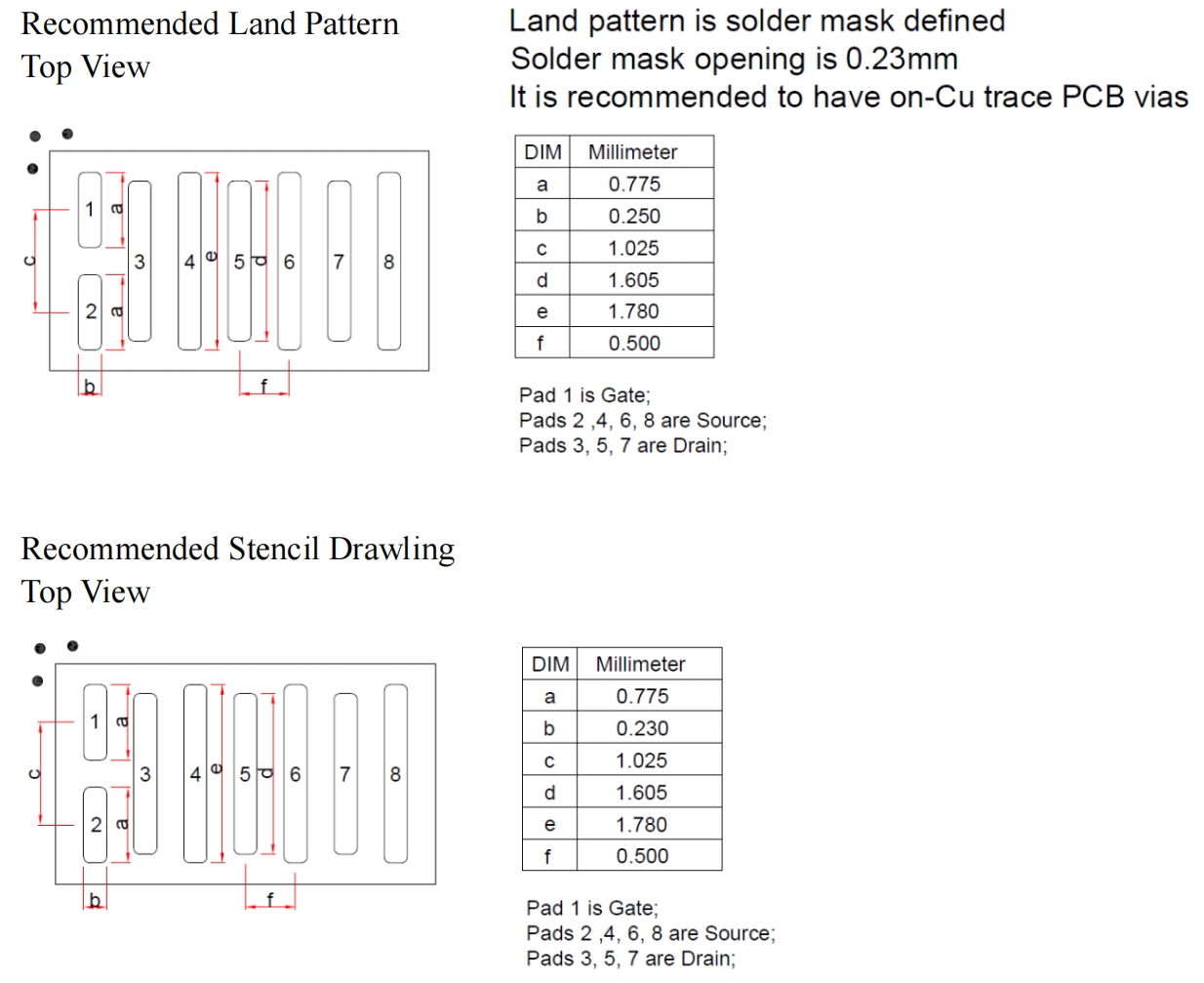
Package Reference
Land Pattern


.jpg?x-oss-process=image/resize,w_100/quality,q_100)
.jpg?x-oss-process=image/resize,w_100/quality,q_100)
.jpg?x-oss-process=image/resize,w_100/quality,q_100)