


.jpg?x-oss-process=image/resize,w_100/quality,q_100)

YZPST-RGN040C024


.jpg)
Pin information
|
Pin |
Pin description |
Pin function |
|
1, 2, 24, 25 |
Gate |
Driver Gate |
|
3-7, 9, 11-20, 22 |
Source |
Source |
|
8, 10, 21, 23 |
Drain |
Power Drain |
Key performance parameters at TJ = 25 °C
|
Parameter |
Value |
Unit |
|
VDS,max |
40 |
V |
|
RDS(on),max @ VGS = 5 V |
4.3 |
mΩ |
|
QG,typ @ VDS = 20V |
6.2 |
nC |
|
IDS,Pulse |
160 |
A |
|
QOSS@ VDS = 20V |
14 |
nC |
Maximum Ratings at TJ = 25 °C unless otherwise specified.
|
SYMBOL |
PARAMETER |
MAX |
UNIT |
|
VDS |
Drain-to-Source Voltage (Continuous) |
40 |
V |
|
ID |
Continuous current |
24 |
A |
|
Pulsed (25˚C, TPulse = 300 µs) |
160 |
A |
|
|
VGS |
Gate-to-Source Voltage |
6 |
V |
|
Gate-to-Source Voltage |
-4 |
V |
|
|
Ptot |
Power dissipation (Tc, bottom = 25°C) |
43 |
W |
|
TJ |
Operating Temperature |
-40 to 150 |
˚C |
|
TSTG |
Storage Temperature |
-40 to 150 |
˚C |
Thermal Characteristics
|
SYMBOL |
PARAMETER |
TYP |
UNIT |
Note/Test Condition |
|
RθJC_top |
Thermal Resistance, Junction to Case (top) |
26.2 |
˚C/W |
|
|
RθJC_bot |
Thermal Resistance, Junction to Case (bottom) |
2.9 |
˚C/W |
|
|
RθJA |
Thermal Resistance, Junction to Ambient 1 |
45.9 |
˚C/W |
|
|
Tsold |
Maximum reflow soldering temperature |
260 |
°C |
MSL3 |
Electric Characteristics at TJ = 25 °C, unless specified otherwise
|
SYMBOL |
PARAMETER |
MIN |
TYP |
MAX |
UNIT |
TEST CONDITIONS |
|
BVDSS |
Drain-to-Source Voltage |
40 |
|
|
V |
VGS = 0 V, ID = 500 μA |
|
IDSS |
Drain Source Leakage |
|
|
100 |
µA |
VGS = 0 V, VDS = 32 V |
|
IGSS |
Gate-to-Source Forward Leakage |
|
3 |
80 |
µA |
VGS = 5 V |
|
Gate-to-Source Forward Leakage |
|
50 |
500 |
µA |
VGS = 5 V, Tj = 125 °C |
|
|
Gate-to-Source Reverse Leakage |
|
1 |
20 |
µA |
VGS = -4 V |
|
|
VGS(TH) |
Gate Threshold Voltage |
0.7 |
|
2.4 |
V |
VDS = VGS , ID = 7 mA |
|
RDS(on) |
Drain-Source On-state Resistance |
|
3 |
4.3 |
mΩ |
VGS = 5 V, ID = 15 A |
|
VSD |
Source-Drain Forward Voltage |
|
1.9 |
|
V |
IS = 0.5 A, VGS = 0 V |
Dynamic characteristics
|
SYMBOL |
PARAMETER |
MIN |
TYP |
MAX |
UNIT |
TEST CONDITIONS |
|
Ciss |
Input Capacitance |
|
805 |
|
pF |
VGS = 0 V, VDS = 20 V |
|
Coss |
Output Capacitance |
|
428 |
|
||
|
Crss |
Reverse Transfer Capacitance |
|
13 |
|
||
|
Coss(er) |
Energy Related Coss |
|
600 |
|
VGS = 5 V, VDS = 20 V, ID=15 A |
|
|
Coss(tr) |
Time Related Coss |
|
703 |
|
||
|
RG |
Gate resistance |
|
1.7 |
|
Ω |
f = 1 MHz |
|
QG |
Total Gate Charge |
|
6.2 |
8.5 |
nC |
VGS = 5 V, VDS = 20 V, ID=15 A |
|
QGS |
Gate to Source Charge |
|
1.4 |
|
VDS = 20 V, ID =15 A |
|
|
QGD |
Gate to Drain Charge |
|
0.8 |
|
||
|
QG(TH) |
Gate Charge at Threshold |
|
0.9 |
|
||
|
QOSS |
Output Charge |
|
14 |
|
VGS = 0 V, VDS = 0 V to 20 V |
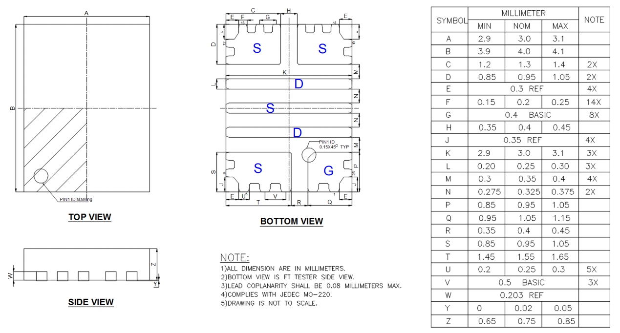
Package Outlines


.jpg?x-oss-process=image/resize,w_100/quality,q_100)
.jpg?x-oss-process=image/resize,w_100/quality,q_100)
.jpg?x-oss-process=image/resize,w_100/quality,q_100)
.jpg?x-oss-process=image/resize,w_100/quality,q_100)