


.jpg?x-oss-process=image/resize,w_100/quality,q_100)
.jpg?x-oss-process=image/resize,w_100/quality,q_100)
.jpg?x-oss-process=image/resize,w_100/quality,q_100)
.jpg?x-oss-process=image/resize,w_100/quality,q_100)


YZPST-RGN800C05D5


.jpg)
Pin information
|
Gate |
Drain |
Kelvin Source |
Source |
|
8 |
1, 2, 3, 4 |
7 |
5, 6, 9 |
Key performance parameters at Tj = 25 °C
|
Parameter |
Value |
Unit |
|
VDS,max |
800 |
V |
|
RDS(on),max @ VGS = 6 V |
480 |
mΩ |
|
QG,typ @ VDS = 400 V |
1.3 |
nC |
|
ID,pulse |
9 |
A |
|
QOSS @ VDS = 400 V |
10.5 |
nC |
|
Qrr @ VDS = 400 V |
0 |
nC |
Maximum ratings at Tj = 25 °C unless otherwise specified.
|
Parameter |
Symbol |
Values |
Unit |
Note/Test Condition |
|
Drain source voltage |
VDS, max |
800 |
V |
VGS = 0 V, Tj = -55 °C to 150 °C |
|
Drain source voltage transient 1 |
VDS, transient |
800 |
V |
VGS = 0 V |
|
Drain source voltage, pulsed 2 |
VDS, pulse |
750 |
V |
Tj = 25 °C; total time < 10 h |
|
Tj = 125 °C; total time < 1 h |
||||
|
Continuous current, drain source |
ID |
5 |
A |
Tc = 25 °C |
|
Pulsed current, drain source 3 |
ID, pulse |
9 |
A |
Tc = 25 °C; VGS = 6 V; tPULSE = 10 µs |
|
Pulsed current, drain source 3 |
ID, pulse |
5 |
A |
Tc = 125 °C; VGS = 6 V; tPULSE = 10 µs |
|
Gate source voltage, continuous 4 |
VGS |
-1.4 to +7 |
V |
Tj = -55 °C to 150 °C |
|
Gate source voltage, pulsed |
VGS, pulse |
-20 to +10 |
V |
Tj = -55 °C to 150 °C; tPULSE = 50 ns, f = 100 kHz; open drain |
|
Power dissipation |
Ptot |
40 |
W |
Tc = 25 °C |
|
Operating temperature |
Tj |
-55 to +150 |
。C |
|
|
Storage temperature |
Tstg |
-55 to +150 |
。C |
Thermal characteristics
|
Parameter |
Symbol |
Values |
Unit |
Note/Test Condition |
|
Thermal resistance, junction-ambient |
RthJA 1 |
72 |
°C/W |
|
|
Thermal resistance, junction-case |
RthJC |
3.05 |
°C/W |
|
|
Thermal resistance, junction-ambient |
Tsold |
260 |
°C |
MSL3 |
Electric characteristics at Tj = 25 °C, unless specified otherwise
|
Parameter |
Symbol |
Values |
Unit |
Note/Test Condition |
||
|
Min. |
Typ. |
Max. |
||||
|
Gate threshold voltage |
VGS(th) |
1.2 |
1.7 |
2.5 |
V |
ID = 5.2 mA; VDS = VGS ; Tj = 25 °C |
|
- |
1.9 |
- |
ID = 5.2 mA; VDS = VGS ; Tj = 150 °C |
|||
|
Drain-source leakage current |
IDSS |
- |
0.2 |
10 |
µA |
VDS = 700 V; VGS = 0 V; Tj = 25 °C |
|
- |
2 |
- |
VDS = 700 V; VGS = 0 V; Tj = 150 °C |
|||
|
Gate-source leakage current |
IGSS |
- |
20 |
- |
µA |
VGS = 6 V; VDS = 0 V |
|
Drain-source on-state resistance |
RDS(on) |
- |
365 |
480 |
mΩ |
VGS = 6 V; ID = 2 A; Tj = 25 °C |
|
- |
790 |
- |
mΩ |
VGS = 6 V; ID = 2 A; Tj = 150 °C |
||
|
Gate resistance |
RG |
- |
14 |
- |
Ω |
f = 5 MHz; open drain |
Dynamic characteristics
|
Parameter |
Symbol |
Values |
Unit |
Note/Test Condition |
||
|
Min. |
Typ. |
Max. |
||||
|
Input capacitance |
Ciss |
- |
43 |
- |
pF |
VGS = 0 V; VDS = 400 V; f = 100 kHz |
|
Output capacitance |
Coss |
- |
13 |
- |
pF |
VGS = 0 V; VDS = 400 V; f = 100 kHz |
|
Reverse transfer capacitance |
Crss |
- |
0.1 |
- |
pF |
VGS = 0 V; VDS = 400 V; f = 100 kHz |
|
Effective output capacitance, energy related 1 |
Co(er) |
- |
18 |
- |
pF |
VGS = 0 V; VDS = 0 to 400 V |
|
Effective output capacitance, time related 2 |
Co(tr) |
- |
26 |
- |
pF |
VGS = 0 V; VDS = 0 to 400 V |
|
Output charge |
QOSS |
- |
10.5 |
- |
nC |
VGS = 0 V; VDS = 0 to 400 V |
|
Turn-on delay time |
td(on) |
- |
2 |
- |
ns |
VDS = 400 V; ID = 4 A; L = 318 µH; VGS = 6 V; Ron = 10 Ω; Roff = 2 Ω; See Figure 22 |
|
Turn-off delay time |
td(off) |
- |
3 |
- |
ns |
|
|
Rise time |
tr |
- |
5 |
- |
ns |
|
|
Fall time |
tf |
- |
7 |
- |
ns |
|
Gate charge characteristics
|
Parameter |
Symbol |
Values |
Unit |
Note/Test Condition |
||
|
Min. |
Typ. |
Max. |
||||
|
Gate charge |
QG |
- |
1.3 |
- |
nC |
VGS = 0 to 6 V; VDS = 400 V; ID = 2 A |
|
Gate-source charge |
QGS |
- |
0.1 |
- |
nC |
|
|
Gate-drain charge |
QGD |
- |
0.5 |
- |
nC |
|
|
Gate Plateau Voltage |
VPlat |
- |
2.7 |
- |
V |
VDS = 400 V; ID = 2 A |
Reverse conduction characteristics
|
Parameter |
Symbol |
Values |
Unit |
Note/Test Condition |
||
|
Min. |
Typ. |
Max. |
||||
|
Source-Drain reverse voltage |
VSD |
- |
2.8 |
- |
V |
VGS = 0 V; IS = 2 A |
|
Pulsed current, reverse |
IS, pulse |
- |
- |
9 |
A |
VGS = 6 V; tPULSE = 10 µs |
|
Reverse recovery charge |
Qrr |
- |
0 |
- |
nC |
IS =2 A; VDS = 400 V |
|
Reverse recovery time |
trr |
- |
0 |
- |
ns |
|
|
Peak reverse recovery current |
Irrm |
- |
0 |
- |
A |
|
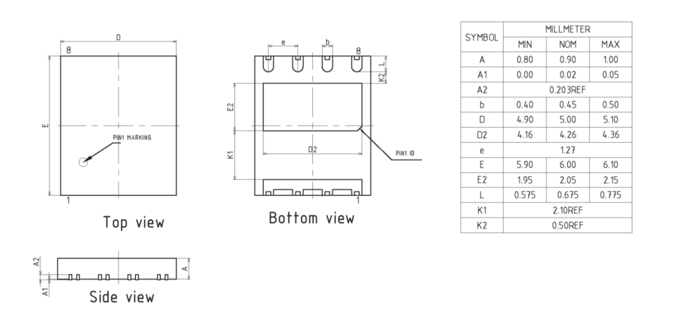
Package outlines
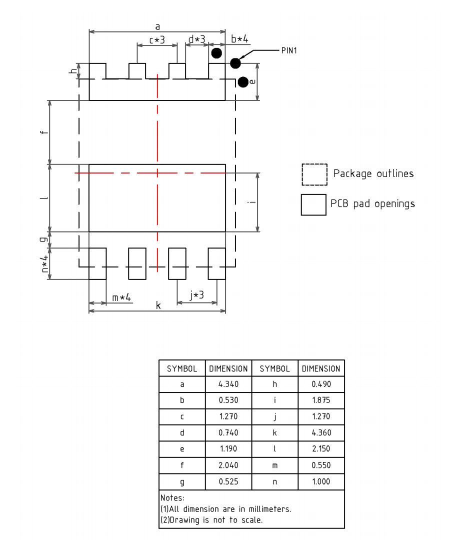
Recommended PCB footprint


.jpg?x-oss-process=image/resize,w_100/quality,q_100)

.jpg?x-oss-process=image/resize,w_100/quality,q_100)
.jpg?x-oss-process=image/resize,w_100/quality,q_100)