


.jpg?x-oss-process=image/resize,w_100/quality,q_100)
.jpg?x-oss-process=image/resize,w_100/quality,q_100)
.jpg?x-oss-process=image/resize,w_100/quality,q_100)
.jpg?x-oss-process=image/resize,w_100/quality,q_100)

YZPST-M1A080120L1
N-Channel SiC Power MOSFET
P/N: YZPST-M1A080120L1
Features
High Blocking Voltage with Low On-Resistance
High Speed Switching with Low Capacitance
Easy to Parallel and Simple to Drive
Benefits
Higher System Efficiency
Reduced Cooling Requirements
Increased Power Density
Increased System Switching Frequency
Applications
Power Supplies
High Voltage DC/DC Converters
Motor Drives
Switch Mode Power Supplies
Pulsed Power applications


description1
Zipper closure
1/5 zip athletic pullovers for men. Stretchy, lightweight, fast-drying
fabric for superior performance.
REGULAR FIT - US standard sizes. An athletic fit that sits close to the
body
for a wide range of motion, designed for optimal performance and all day
comfort.
FEATURES - Quarter zip closure;Thumbholes on long sleeves to keep them
in
place during workout
DESCRIPTION

N-Channel SiC Power MOSFET
P/N: YZPST-M1A080120L1
Features
High Blocking Voltage with Low On-Resistance
High Speed Switching with Low Capacitance
Easy to Parallel and Simple to Drive
Benefits
Higher System Efficiency
Reduced Cooling Requirements
Increased Power Density
Increased System Switching Frequency
Applications
Power Supplies
High Voltage DC/DC Converters
Motor Drives
Switch Mode Power Supplies
Pulsed Power applications

|
Part Number |
Package |
|
M1A080120 L1 |
TO-247-4 |
Maximum Ratings (TC=25℃ unless otherwise specified)
| Symbol | Parameter | Value | Unit | Test Conditions | Note |
| VDSmax | Drain-Source Voltage | 1200 | V | VGS=0V, ID=100μA | |
| VGSmax | Gate-Source Voltage | -0.4 | V | Absolute maximum values | |
| VGSop | Gate-Source Voltage | -0.25 | V | Recommended operational values | |
| ID | Continuous Drain Current | 36 | A | VGS=20V, Tc=25℃ | |
| 24 | VGS=20V, Tc=100℃ | ||||
| ID(pulse) | Pulsed Drain Current | 80 | A | Pulse width tp limited by TJmax | |
| PD | Power Dissipation | 192 | W | Tc=25℃, TJ=150℃ | |
| TJ, TSTG | Operating Junction and Storage Temperature | -55 to +150 | ℃ |
Electrical Characteristics (TC=25℃ unless otherwise specified)
| Symbol | Parameter | Min. | Typ. | Max. | Unit | Test Conditions | Note |
| V(BR)DSS | Drain-Source Breakdown Voltage | 1200 | / | / | V | VGS=0V, ID=100μA | |
| VGS(th) | Gate Threshold Voltage | 2 | 2.4 | 4 | V | VDS=VGS, ID=5mA | Fig. 11 |
| / | 1.8 | / | VDS=VGS, ID=5mA, TJ=150℃ | ||||
| IDSS | Zero Gate Voltage Drain Current | / | 1 | 100 | µA | VDS=1200V, VGS=0V | |
| IGSS+ | Gate-Source Leakage Current | / | 10 | 250 | nA | VDS=0V, VGS=25V | |
| IGSS- | Gate-Source Leakage Current | / | 10 | 250 | nA | VDS=0V, VGS=-10V | |
| RDS(on) | Drain-Source On-State Resistance | / | 80 | 98 | mΩ | VGS=20V, ID=20A | Fig. |
| / | 140 | / | VGS=20V, ID=20A, TJ=150℃ | 4,5,6 | |||
| Ciss | Input Capacitance | / | 1475 | / | VGS=0V | Fig. | |
| Coss | Output Capacitance | / | 94 | / | pF | VDS=1000V | 15,16 |
| Crss | Reverse Transfer Capacitance | / | 11 | / | f=1MHz | ||
| Eoss | Coss Stored Energy | / | 52 | / | µJ | VAC=25mV | |
| EON | Turn-On Switching Energy | / | 564 | / | µJ | VDS=800V, VGS=-5V/20V | |
| EOFF | Turn-Off Switching Energy | / | 260 | / | ID=20A, RG(ext)=2.5Ω, L=200μH | ||
| td(on) | Turn-On Delay Time | / | 9.3 | / | |||
| tr | Rise Time | / | 9.5 | / | VDS=800V, VGS=-5V/20V, ID=20A RG(ext)=2.5Ω, RL=40Ω | ||
| td(off) | Turn-Off Delay Time | / | 18 | / | ns | ||
| tf | Fall Time | / | 7.6 | / | |||
| RG(int) | Internal Gate Resistance | / | 3.1 | / | Ω | f=1MHz, VAC=25mV | |
| QGS | Gate to Source Charge | / | 24 | / | VDS=800V | ||
| QGD | Gate to Drain Charge | / | 15 | / | nC | VGS=-5V/20V | |
| QG | Total Gate Charge | / | 79 | / | ID=20A |
Reverse Diode Characteristics
| Symbol | Parameter | Typ. | Max. | Unit | Test Conditions | Note |
| VSD | Diode Forward Voltage | 3.6 | / | V | VGS=-5V, ISD=10A | Fig. 8,9,10 |
| 3.3 | / | VGS=-5V, ISD=10A, TJ=150℃ | ||||
| IS | Continuous Diode Forward Current | / | 44 | A | TC=25℃ | |
| trr | Reverse Recover Time | 35 | / | ns | ||
| Qrr | Reverse Recovery Charge | 91 | / | nC | VR=800V, ISD=20A | |
| Irrm | Peak Reverse Recovery Current | 4.5 | / | A |
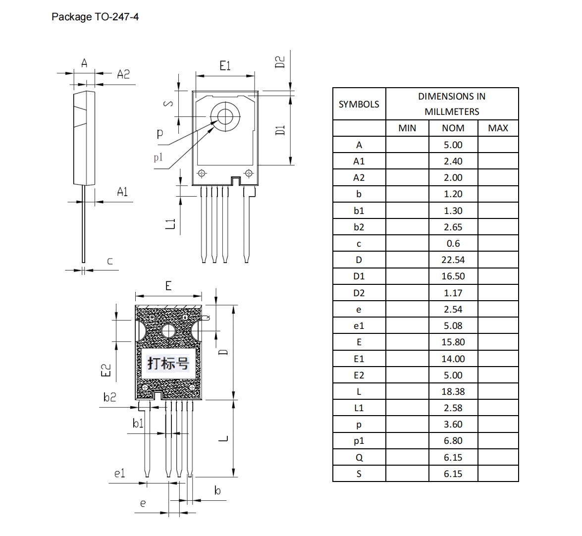
Package Dimensions
Package TO-247-4
Related Products


.jpg?x-oss-process=image/resize,w_100/quality,q_100)


.jpg?x-oss-process=image/resize,w_100/quality,q_100)

.jpg?x-oss-process=image/resize,w_100/quality,q_100)

.jpg?x-oss-process=image/resize,w_100/quality,q_100)

.webp?x-oss-process=image/resize,w_100/quality,q_100)
