


.jpg?x-oss-process=image/resize,w_100/quality,q_100)
.jpg?x-oss-process=image/resize,w_100/quality,q_100)
.jpg?x-oss-process=image/resize,w_100/quality,q_100)
.jpg?x-oss-process=image/resize,w_100/quality,q_100)

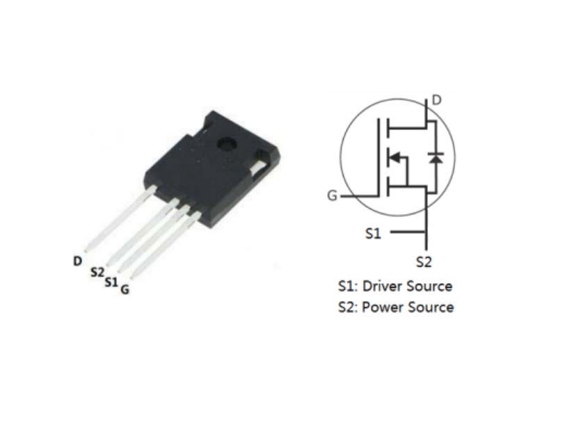
YZPST-M1A045170L
P/N:YZPST-M1A045170L
Silicon Carbide Power MOSFET
( N Channel Enhancement Mode)
Features
High Speed Switching with Low Capacitances
High Blocking Voltage with Low On-Resistance
Easy to Parallel and Simple to Drive
Resistant to Latch-UP
Halogen Free, RoHS Compliant
Benefits
Higher System Efficiency
Reduced Cooling Requirements
Increased Power Density
Increased System Switching Frequency
Applications
Solar Inverters
Switch Mode Power Supplies
High Voltage DC/DC Converters
Motor Drive

description1
Zipper closure
1/5 zip athletic pullovers for men. Stretchy, lightweight, fast-drying
fabric for superior performance.
REGULAR FIT - US standard sizes. An athletic fit that sits close to the
body
for a wide range of motion, designed for optimal performance and all day
comfort.
FEATURES - Quarter zip closure;Thumbholes on long sleeves to keep them
in
place during workout
DESCRIPTION

P/N:YZPST-M1A045170L
Silicon Carbide Power MOSFET
( N Channel Enhancement Mode)
Features
High Speed Switching with Low Capacitances
High Blocking Voltage with Low On-Resistance
Easy to Parallel and Simple to Drive
Resistant to Latch-UP
Halogen Free, RoHS Compliant
Benefits
Higher System Efficiency
Reduced Cooling Requirements
Increased Power Density
Increased System Switching Frequency
Applications
Solar Inverters
Switch Mode Power Supplies
High Voltage DC/DC Converters
Motor Drive
|
Part Number |
Package |
Marking |
|
M1A045170L |
TO-247-4L |
M1A045170L |
Maximum Ratings (Tc = 25°C unless otherwise specified)
| Symbol | Parameter | Value | Unit | Test Conditions | Note |
| VDSmax | Drain-Source Voltage | 1700 | V | VGS = 0 V, ID = 100 μA | |
| VGSmax | Gate-Source Voltage | -0.4 | V | Absolute maximum values | |
| VGSop | Gate-Source Voltage | -0.25 | V | Recommended operational values | |
| ID | Continuous Drain Current | 85 | A | VGS = 20 V, TC = 25˚C | |
| 55 | VGS = 20 V, TC = 100˚C | ||||
| ID(pluse) | Pulsed Drain Current | 160 | A | Pulse width tP limited by Tjmax | |
| PD | Power Dissipation | 520 | W | TC =25˚C, TJ =150℃ | |
| TJ , Tstg | Operating Junction and Storage Temperature | -55 to 175 | ℃ | ||
| TL | Solder Temperature | 260 | ℃ | 1.6mm (0.063 ”) from case for 10s | |
| Md | Mounting Torque | 1 | Nn | M3 or 6-32 screw | |
| 8.8 | lbf-in |
Electrical Characteristics (Tc = 25°C unless otherwise specified)
| Symbol | Parameter | Min. | Typ. | Max. | Unit | Test Conditions | Note | |
| V(BR)DSS | Drain Drain-Source | 1700 | - | V | VGS = 0 V, ID = 100 μA | |||
| Breakdown Voltage | ||||||||
| 2 | 2.6 | 4 | V | VDS = VGS, ID = 18mA | ||||
| VGS(th) | Gate threshold Voltage | 1.9 | V | VDS = VGS, ID = 18mA, TJ =150°C | ||||
| IDSS | Zero Gate Voltage Drain Current | 2 | 100 | μA | VDS = 1700 V, VGS = 0 V | |||
| IGSS | Gate Source Leakage | 2 | uA | VGS = 20 V, VDS = 0 V | ||||
| Current | ||||||||
| Drain-Source | 34 | 60 | mΩ | VGS = 20 V, ID = 50 A | ||||
| RDSON | On-State Resistance | 66 | VGS = 20 V, ID = 50A, TJ =150°C | |||||
| gfs | Transconductance | 16 | VGS = 20 V, ID = 50A | |||||
| 19 | S | VGS = 20 V, ID = 50A, TJ =150°C | ||||||
| C | Input Capacitance | 4078 | ||||||
| oss | Output Capacitance | 167 | ||||||
| rss | Reverse Capacitance | 39 | pF | VDS =1000V,TJ=25°C,f=1MHz | ||||
| Eoss | Coss Stored Energy | 203 | μJ | |||||
| Eon | Turn on Switching Energy | 1.9 | VDS = 1200 V, VGS = -5/20 V, ID = 50A, Rg(ext) = 2.5Ω, | |||||
| Eoff | Turn off Switching Energy | 0.3 | mJ | TJ=150°C | ||||
| tdon | Turn on delay time | 21 | ||||||
| tr | Rise time | 46 | VDS = 1200 V, VGS = -5/20 V, ID = 50A, Rg(ext)= 2.5Ω | |||||
| tdoff | Turn off delay time | 50 | ||||||
| tf | Fall time | 19 | ns | |||||
| Rgint | Internal Gate Resistance | 2.6 | VAC =25mV, f=1MHz | |||||
| Qgs | Gate to Source Charge | 44 | VDS = 1200 V, VGS = -5/20 V, ID = 50A | |||||
| Qgd | Gate to Drain Charge | 84 | ||||||
| Qg | Total Gate Charge | 248 | nC |
Electrical Characteristics (Tc = 25°C unless otherwise specified)
| Symbol | Parameter | Min. | Typ. | Max. | Unit | Test Conditions | Note |
| VSD | Diode Forward Voltage | 6.1 | - | V | VGS = -5 V, ISD = 25 A | ||
| 5.2 | VGS = -5 V, ISD = 25 A,TJ =150°C | ||||||
| I | Continuous Diode Forward Current | 75 | A | VGS = -5V, Tc=25°C | |||
| S | |||||||
| trr | Reverse Recovery Time | 126 | ns | VR= 1200 V, VGS = -5V, ID = 50A, di/dt=1400A/μS,, TJ =150°C | |||
| Qrr | Reverse Recovery Charge | 1360 | nC | ||||
| Irrm | Peak Reverse Recovery Current | 19 | A |

Related Products


.jpg?x-oss-process=image/resize,w_100/quality,q_100)
.jpg?x-oss-process=image/resize,w_100/quality,q_100)


.jpg?x-oss-process=image/resize,w_100/quality,q_100)

.jpg?x-oss-process=image/resize,w_100/quality,q_100)

.webp?x-oss-process=image/resize,w_100/quality,q_100)
